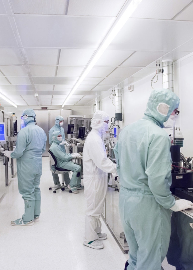
Manufacturing
Made for the consumer market
Our waveguide technology was designed from the outset with mass manufacture in mind. Our structures are technically sophisticated, but physically simple, which makes manufacturing using standard nano-imprinting methods possible.
Mass Manufacturing of Diffractive Waveguides
WaveOptics has designed a simple manufacturing process, which enables our waveguides to be mass produced at low cost. We use standard, high volume capable tools to ensure that low-cost, high yield manufacture is possible. Our dedicated manufacturing line is situated at Goertek’s state of the art facility in Weifang, China where we have WaveOptics team members on site to support.
Nanoimprinting Lithography
Mass production of waveguides on glass wafers
Optical Coating
Optical coatings are deposited on the wafers
Laser Cutting
Individual waveguides are cut from the wafers
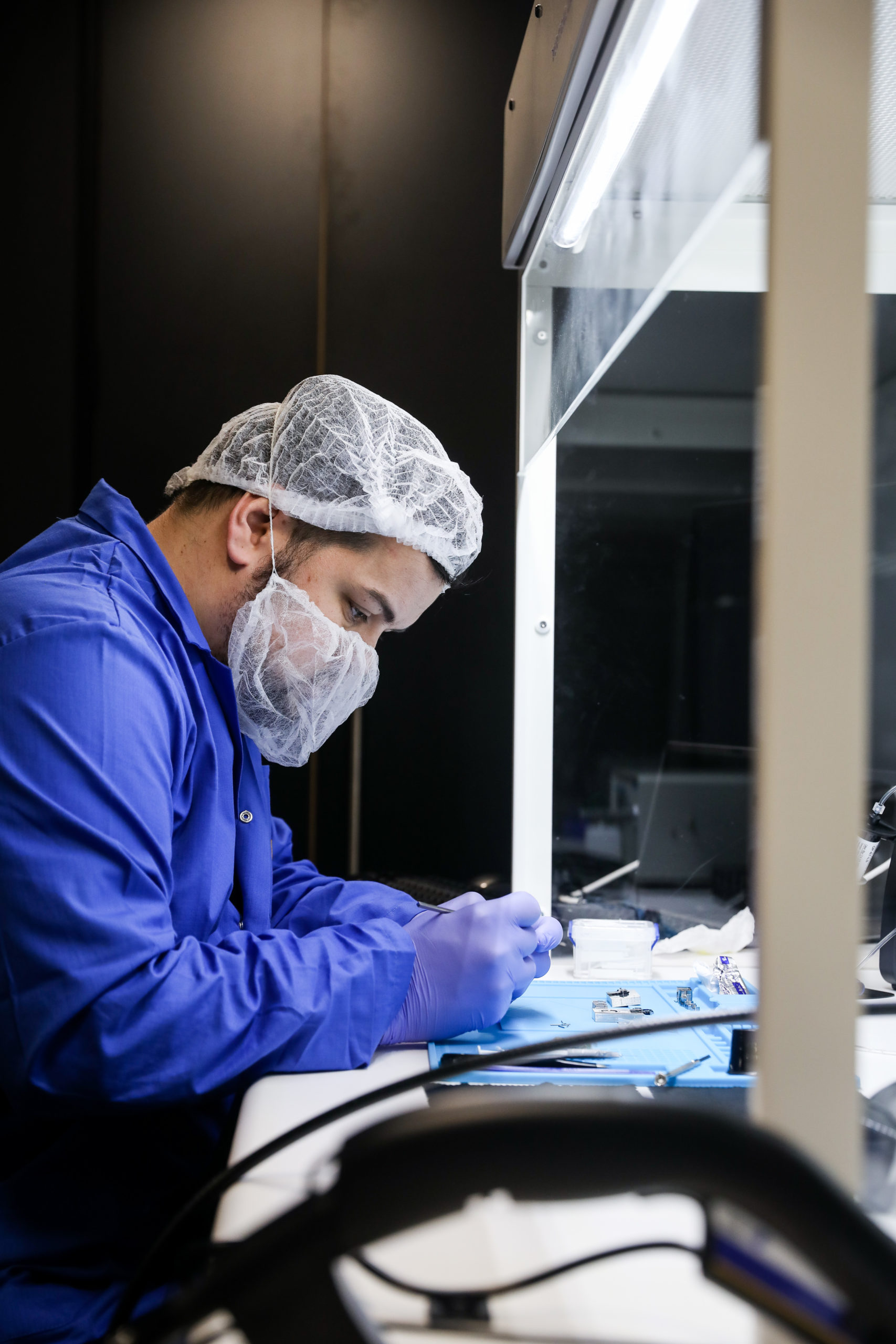
Assembly
Individual waveguides are aligned and fixed together
Edge Blackening
Tinted to enhance image quality
Characterisation
All waveguide assemblies are tested for accuracy and optical performance


Manufacturing of Projectors
Projectors are critical to the performance of the overall AR system. We have designed our projectors to be compact and efficient. We believe that by taking control of this critical component we can guarantee the supply and performance of the AR system. Our in-house capabilities have allowed us to create a range of DMD, LCoS and Micro-LED based projectors to complement and enhance our waveguide portfolio.
Assemble lens barrel
Optical components assembled into housing
Assemble projector body
LEDs, optical components and DMD/LCoS aligned and assembled into main body
Attach barrel to projector body
Barrel assembly aligned and focused to projector image
Test and inspect
All projector assemblies tested for optical performance
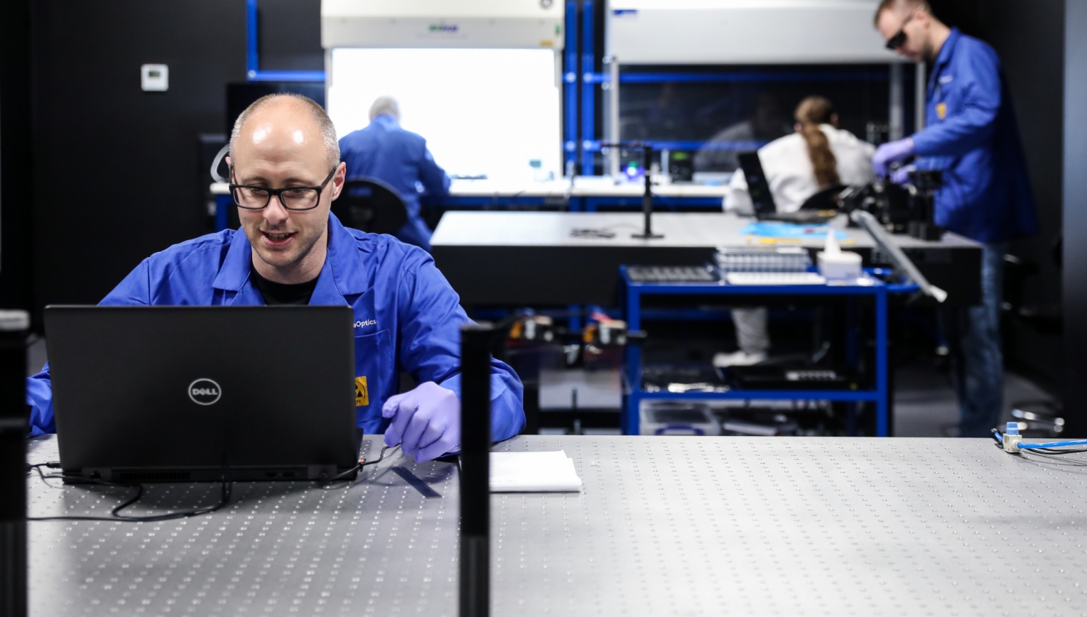
Prototyping Facility
We have installed a dedicated UK based prototype facility.
It has a waveguide assembly line, that includes waveguide stacking, edge blackening & testing. There is dedicated space for projector assembly and optical engine assembly, where we are able to test out designs and prototypes. This helps speed up the product design process for WaveOptics standard products, as well as customer projects.
The secure facility will also be used for training our contract manufacturing and ODM partners. The facility is a unique space where our partners can learn quickly how best to build and align WaveOptics’ optical engines. This will enable the transfer of this skill set into our partners’ own manufacturing environments.
The prototyping facility also has additional dedicated lab space to support our R&D efforts, focused particularly on new technologies.
State of the art equipment enables our teams to rapidly evaluate and test new R&D approaches.